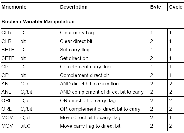
ALU (arithmetic/logic unit)
Performs arithmetic functions such as add,
subtract, multiply, and divide, and logic
functions such as AND, OR, and NOT
Program counter
Points to the address of the next
instruction to be executed
As each instruction is executed, the program
counter is incremented to point to the address
of the next instruction to be executed
Instruction decoder
Interprets the instruction fetched into the
CPU
A CPU capable of understanding more
instructions requires more transistors to design
Tuesday, November 9, 2010
Registers
Registers
The CPU uses registers to store
information temporarily
Values to be processed
Address of value to be fetched from memory
In general, the more and bigger the
registers, the better the CPU
Registers can be 8-, 16-, 32-, or 64-bit
The disadvantage of more and bigger registers
is the increased cost of such a CPU

INSIDE THE COMPUTER
Important Terminology
The unit of data size
Bit : a binary digit that can have the value
0 or 1
Byte : 8 bits
Nibble : half of a bye, or 4 bits
Word : two bytes, or 16 bits
The terms used to describe amounts of
memory in IBM PCs and compatibles
Kilobyte (K): 210 bytes
Megabyte (M) : 220 bytes, over 1 million
Gigabyte (G) : 230 bytes, over 1 billion
Terabyte (T) : 240 bytes, over 1 trillion
Internal Organization of Computers
CPU (Central Processing Unit)
Execute information stored in memory
I/O (Input/output) devices
Provide a means of communicating with
CPU
Memory
RAM (Random Access Memory) –
temporary storage of programs that
computer is running
The data is lost when computer is off
ROM (Read Only Memory) – contains
programs and information essential to
operation of the computer
The information cannot be changed by use,
and is not lost when power is off
– It is called nonvolatile memory

The CPU is connected to memory and
I/O through strips of wire called a bus
Carries information from place to place
Address bus
Data bus
Control bus

better the CPU
Think of data buses as highway lanes
More data buses mean a more
expensive CPU and computer
The average size of data buses in CPUs
varies between 8 and 64
Data buses are bidirectional
To receive or send data
The processing power of a computer is
related to the size of its buses
The more address buses available, the
larger the number of devices that can
be addressed
The number of locations with which a
CPU can communicate is always equal
to 2x, where x is the address lines,
regardless of the size of the data bus
ex. a CPU with 24 address lines and 16
data lines can provide a total of 224 or 16M
bytes of addressable memory
Each location can have a maximum of 1
byte of data, since all general-purpose
CPUs are byte addressable
The address bus is unidirectional
CPU’s Relation to RAM and ROM
For the CPU to process information,
the data must be stored in RAM or
ROM, which are referred to as primary
memory
ROM provides information that is fixed
and permanent
Tables or initialization program
RAM stores information that is not
permanent and can change with time
Various versions of OS and application
packages
CPU gets information to be processed
first form RAM (or ROM)
if it is not there, then seeks it from a mass
storage device, called secondary memory, and
transfers the information to RAM
The unit of data size
Bit : a binary digit that can have the value
0 or 1
Byte : 8 bits
Nibble : half of a bye, or 4 bits
Word : two bytes, or 16 bits
The terms used to describe amounts of
memory in IBM PCs and compatibles
Kilobyte (K): 210 bytes
Megabyte (M) : 220 bytes, over 1 million
Gigabyte (G) : 230 bytes, over 1 billion
Terabyte (T) : 240 bytes, over 1 trillion
Internal Organization of Computers
CPU (Central Processing Unit)
Execute information stored in memory
I/O (Input/output) devices
Provide a means of communicating with
CPU
Memory
RAM (Random Access Memory) –
temporary storage of programs that
computer is running
The data is lost when computer is off
ROM (Read Only Memory) – contains
programs and information essential to
operation of the computer
The information cannot be changed by use,
and is not lost when power is off
– It is called nonvolatile memory

The CPU is connected to memory and
I/O through strips of wire called a bus
Carries information from place to place
Address bus
Data bus
Control bus

Address bus
For a device (memory or I/O) to be
recognized by the CPU, it must be
assigned an address
The address assigned to a given device must
be unique
The CPU puts the address on the address bus,
and the decoding circuitry finds the device
Data bus
The CPU either gets data from the device
or sends data to it
Control bus
Provides read or write signals to the
device to indicate if the CPU is asking for
information or sending it information
The more data buses available, the
better the CPU
Think of data buses as highway lanes
More data buses mean a more
expensive CPU and computer
The average size of data buses in CPUs
varies between 8 and 64
Data buses are bidirectional
To receive or send data
The processing power of a computer is
related to the size of its buses
The more address buses available, the
larger the number of devices that can
be addressed
The number of locations with which a
CPU can communicate is always equal
to 2x, where x is the address lines,
regardless of the size of the data bus
ex. a CPU with 24 address lines and 16
data lines can provide a total of 224 or 16M
bytes of addressable memory
Each location can have a maximum of 1
byte of data, since all general-purpose
CPUs are byte addressable
The address bus is unidirectional
CPU’s Relation to RAM and ROM
For the CPU to process information,
the data must be stored in RAM or
ROM, which are referred to as primary
memory
ROM provides information that is fixed
and permanent
Tables or initialization program
RAM stores information that is not
permanent and can change with time
Various versions of OS and application
packages
CPU gets information to be processed
first form RAM (or ROM)
if it is not there, then seeks it from a mass
storage device, called secondary memory, and
transfers the information to RAM
Saturday, September 25, 2010


Wednesday, August 25, 2010
Interfacing Relay to 8051
Relays are devices which allow low power circuits to switch a relatively high Current/Voltage ON/OFF. For a relay to operate a suitable pull-in & holding currentshould be passed through its coil. Generally relay coils are designed to operate from a particular voltage often its 5V or 12V.
The function of relay driver circuit is to provide the necessary current (typically 25 to 70ma) to energize the relay coil.
Figure 1 shows the basic relay driver circuit. As you can see an NPN transistor BC547 is being used to control the relay. The transistor is driven into saturation (turned ON) when a LOGIC 1 is written on the PORT PIN thus turning ON the relay. The relay is turned OFF by writing LOGIC 0 on the port pin. A diode (1N4007/1N4148) is connected across the relay coil; this is done so as to protect the transistor from damage due to the BACK EMF generated in the relay's inductive coil when the transistor is turned OFF. When the transistor is switched OFF the energy stored in the inductor is dissipated through the diode & the internal resistance of the relay coil. Normally 1N4148 can be used as it is fast switching diode with a maximum forward current of 300ma. This diode is also called as free-wheeling diode.
The LED is used to indicate that the RELAY has been turned ON. The resistor R1 defines the current flowing through the LED thereby defining the LED’s intensity.
Resistor R2 is used as a Series Base Resistor to set the base current. When working with 8051 controllers I have noted that it’s not compulsory to use this resistor as the controller has internal 10k resistor which acts as a base resistor.Microcontrollers have internal pull up resistors hence when a port pin is HIGH the output current flows through this internal pull up resistor. 8051 microcontrollers have an internal pull up of 10KΩ. Hence the maximum output current will be 5v/10k = 0.5ma. This current is not sufficient to drive the transistor into saturation and turn ON the relay. Hence an external pull up resistor R3 is used. Let us now calculate the value of R3. Normally a relay requires a pull in current of 70ma to be turned ON. So our BC547 transistor will require enough base current to make sure it remains saturated and provide the necessary collector current i.e. 70ma. The gain (hfe) of BC547 is 100 so we need to provide at least 70ma/100 = 0.7ma of base current. In practice you require roughly double the value of this current so we will calculate for 1.4ma of base current.
Base Current(1.4ma) =o/p current of controller (0.5ma) + 5v/R3
From the above equation the value of R3 comes out to be 5.55KΩ. Typically I use 4.7KΩ resistor.
Whenever 8051 microcontroller is turned ON initially the controller is in reset state and all the controller pins are HIGH which would result in TURNING ON the relay every time power is turned ON or if there is a power fluctuation. This may also damage the device connected to relay so as to avoid this problem another transistor Q2 has been added between the controller & the previous transistor. This transistor acts as an inverter.Figure 2 shows the upated Relay Driver Circuit. So now when a High is applied from the controller the TRANSISTOR Q2 turns ON so the base of transistor Q1 gets 0 so the transistor Q1 turns OFF so the relay turns OFF. And when a LOW is applied from the controller the TRANSISTOR Q2 turns OFF so the base of transistor Q1 gets high voltage through the resistor R2 so the transistor Q1 turns ON which turns ON the relay.So basically Q2 & R2 acts as an inverter.

If you want to connect more relays to microcontroller then you can use ULN 2003 for connecting seven relays or ULN 2803 for connecting eight relays. Figure 3 shows how to connect a relay to microcontroller using ULN 2003/ULN 2803. These IC’s are high voltage, high current Darlington transistor arrays with open collector outputs and free-wheeling clamping diodes hence there is no need of a diode across the relay. Also there is no need of the series base resistor as the IC has an internal resistor of 2.7KΩ
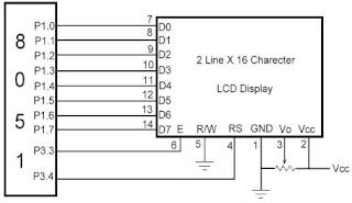
Interfacing LCD to 8051
Liquid Crystal Display also called as LCD is very helpful in providing user interface as well as for debugging purpose. The most common type of LCD controller is HITACHI 44780 which provides a simple interface between the controller & an LCD. These LCD's are very simple to interface with the controller as well as are cost effective.
The most commonly used ALPHANUMERICdisplays are 1x16 (Single Line & 16 characters), 2x16 (Double Line & 16 character per line) & 4x20 (four lines & Twenty characters per line).

When RS is low (0), the data is to be treated as a command. When RS is high (1), the data being sent is considered as text data which should be displayed on the screen.
When R/W is low (0), the information on the data bus is being written to the LCD. When RW is high (1), the program is effectively reading from the LCD. Most of the times there is no need to read from the LCD so this line can directly be connected to Gnd thus saving one controller line.
The ENABLE pin is used to latch the data present on the data pins. A HIGH - LOW signal is required to latch the data. The LCD interprets and executes our command at the instant the EN line is brought low. If you never bring EN low, your instruction will never be executed.
 For Contrast setting a 10K pot should be used as shown in the figure.
Display Data Ram (DDRAM) stores the display data. So when we have to display a character on LCD we basically write it into DDRAM. For a 2x16 LCD the DDRAM address for first line is from 80h to 8fh & for second line is 0c0h to 0cfh. So if we want to display 'H' on the 7th postion of the first line then we will write it at location 87h.
Now as you have noticed two types of data is given to the LCD data to be displayed, command or special instruction.So now let us write a subroutine for both the type of data

Before starting to display on LCD we need to Initialize it. Firstly we must tell the LCD whether we'll be using 8-bit or 4-bit mode. Also we will be telling the LCD that we need 5x8 character font. Both these options are selected using a single command i.e. 38h. So to activate both these options we must execute following instructions:
The most commonly used ALPHANUMERICdisplays are 1x16 (Single Line & 16 characters), 2x16 (Double Line & 16 character per line) & 4x20 (four lines & Twenty characters per line).

The LCD requires 3 control lines (RS, R/W & EN) & 8 (or 4) data lines. The number on data lines depends on the mode of operation. If operated in 8-bit mode then 8 data lines + 3 control lines i.e. total 11 lines are required. And if operated in 4-bit mode then 4 data lines + 3 control lines i.e. 7 lines are required. How do we decide which mode to use? It’s simple if you have sufficient data lines you can go for 8 bit mode & if there is a time constrain i.e. display should be faster then we have to use 8-bit mode because basically 4-bit mode takes twice as more time as compared to 8-bit mode.
| Pin | Symbol | Function |
| 1 | Vss | Ground |
| 2 | Vdd | Supply Voltage |
| 3 | Vo | Contrast Setting |
| 4 | RS | Register Select |
| 5 | R/W | Read/Write Select |
| 6 | En | Chip Enable Signal |
| 7-14 | DB0-DB7 | Data Lines |
| 15 | A/Vee | Gnd for the backlight |
| 16 | K | Vcc for backlight |
When RS is low (0), the data is to be treated as a command. When RS is high (1), the data being sent is considered as text data which should be displayed on the screen.
When R/W is low (0), the information on the data bus is being written to the LCD. When RW is high (1), the program is effectively reading from the LCD. Most of the times there is no need to read from the LCD so this line can directly be connected to Gnd thus saving one controller line.
The ENABLE pin is used to latch the data present on the data pins. A HIGH - LOW signal is required to latch the data. The LCD interprets and executes our command at the instant the EN line is brought low. If you never bring EN low, your instruction will never be executed.

Display Data Ram (DDRAM) stores the display data. So when we have to display a character on LCD we basically write it into DDRAM. For a 2x16 LCD the DDRAM address for first line is from 80h to 8fh & for second line is 0c0h to 0cfh. So if we want to display 'H' on the 7th postion of the first line then we will write it at location 87h.
Now as you have noticed two types of data is given to the LCD data to be displayed, command or special instruction.So now let us write a subroutine for both the type of data
Data to be Displayed
· lcd_datadisplay:
· SETB RS //Telling the LCD that the data which is being send is to be displayed
· MOV P1,A //Character to be displayed is in Acc
· SETB EN
· CLR EN //High to Low pulse on EN to latch the data
· CALL DELAY //Delay so that LCD finishes its internal operations
· ret
Command or Special Instruction.
Here I have used delay at the end of both the subroutines this is done to wait until the instruction is completely executed by the LCD. This will assure that our program gives the LCD the time it needs to execute instructions and also makes our program compatible with any LCD, regardless of how fast or slow it is.· lcd_command:
· CLR RS //Telling the LCD that the data which is being send is a command
· MOV P1,A //Character to be displayed is in Acc
· SETB EN
· CLR EN //High to Low pulse on EN to latch the data
· CALL DELAY //Delay so that LCD finishes its internal operations
· ret

"*" - Not Used/Ignored. This bit can be either "1" or "0"
Set Cursor Move Direction:
ID - Increment the Cursor After Each Byte Written to Display if Set
S - Shift Display when Byte Written to Display Enable Display/Cursor
D - Turn Display On(1)/Off(0) C - Turn Cursor On(1)/Off(0)
B - Cursor Blink On(1)/Off(0)
Move Cursor/Shift Display
SC - Display Shift On(1)/Off(0) RL - Direction of Shift Right(1)/Left(0)
Set Interface Length
Move Cursor to CGRAM/DisplayDL - Set Data Interface Length 8(1)/4(0)
N - Number of Display Lines 1(0)/2(1)
F - Character Font 5x10(1)/5x7(0)
Poll the "Busy Flag" BF - This bit is set while the LCD is processing
Read/Write ASCII to the DisplayA - Address
The above Table shows the different commands for the LCD. I wont go into its details.D - Data
Before starting to display on LCD we need to Initialize it. Firstly we must tell the LCD whether we'll be using 8-bit or 4-bit mode. Also we will be telling the LCD that we need 5x8 character font. Both these options are selected using a single command i.e. 38h. So to activate both these options we must execute following instructions:
Now that we have to Turn On the display & set the cursor option i.e. cursor ON/OFF & Cursor blinking ON/OFF for that we will use the command 0Eh i.e. Display On , Cursor ON but Cursor blinking OFF.· MOV A,#38h
· CALL lcd_command
And the last command we require is to configure the LCD in such a way that everytime we send a character to it the cursor position automatically increments by one & moves to right i.e. 06h.· MOV A,#0Eh
· CALL lcd_command
So the lcd_initialize contains the following instructions· MOV A,#06h
· CALL lcd_command
Similarly another important instruction that we require is Clearing the LCD i.e.· lcd_initialize:
· MOV A,#38h
· CALL lcd_command
· MOV A,#38h
· CALL lcd_command
· MOV A,#38h
· CALL lcd_command
· ret
Now we know all the commands to display on LCD. Let us write a program that will display 'DNA TECHNOLOGY' on LCD.· lcd_clr:
· MOV A,#01h
· CALL lcd_command
· ret
· ORG 0000h
· CALL lcd_initialize
· CALL lcd_clr
· MOV A,#80h //Location from where Data is to be displayed
· CALL lcd_command
· MOV A,#'D'
· CALL lcd_datadisplay
· MOV A,#'N'
· CALL lcd_datadisplay
· MOV A,#'A'
· CALL lcd_datadisplay
· MOV A,#20h //Hex value for blank space to be displayed
· CALL lcd_datadisplay
· MOV A,#'T'
· CALL lcd_datadisplay
· MOV A,#'E'
· CALL lcd_datadisplay
· MOV A,#'C'
· CALL lcd_datadisplay
· MOV A,#'H'
· CALL lcd_datadisplay
· MOV A,#'N'
· CALL lcd_datadisplay
· MOV A,#'O'
· CALL lcd_datadisplay
· MOV A,#'L'
· CALL lcd_datadisplay
· MOV A,#'O'
· CALL lcd_datadisplay
· MOV A,#'G'
· CALL lcd_datadisplay
· MOV A,#'Y'
· CALL lcd_datadisplay
· stop:
· ajmp stop
Debugging Procedure
If the above program does not work then follow these steps:-1) Check if the supply is correct.
2) If all connections are correct.
3) Increase the delay time.
Interfacing Matrix Keypad to 8051
Before learning “Interfacing Matrix Keypad to Microcontroller” you should know how to interface a switch to microcontroller for which please click here.
As you have seen in the article for interfacing switches to microcontroller normally the port pin is high but when a switch is pressed the controller pin gets a Low signal and we come to know that a switch has been pressed. One end of switch is connected to the port pin whereas the other end is connected to the Ground.
In case of matrix Keypad both the ends of switches are connected to the port Pin. Over here we have considered a 4x3 matrix keypad i.e. four rows and three columns. So in all twelve switches have been interfaced using just seven lines. The adjoining figure shows the diagram of a matrix keypad and how it is interfaced with the controller.

As you can see no pin is connected to ground, over here the controller pin itself provides the ground. We pull one of the Column Pins low & check the row pins if any of the Pin is low then we come to know which switch is pressed.
Suppose we make column 1 pin low and while checking the rows we get Row 3 is low then we come to know switch 7 has been pressed.

ALGORITHM
1. Start.
2. Make All Pins High.
3. Make Column 1 pin low.
4. Check if Row 1 is low, if yes then Switch 1 has been pressed.
5. Check if Row 2 is low, if yes then Switch 4 has been pressed.
6. Check if row 3 is low if yes then Switch 7 has been pressed.
7. Check if row 4 is low if yes then Switch 10 has been pressed.
8. Make Column 1 Pin high & Column 2 Pin Low.
9. Check if Row 1 is low, if yes then Switch 2 has been pressed.
10. Check if Row 2 is low, if yes then Switch 5 has been pressed.
11. Check if row 3 is low if yes then Switch 8 has been pressed.
12. Check if row 4 is low if yes then Switch 11 has been pressed.
13. Make Column 2 Pin high & Column 3 Pin Low.
14. Check if Row 1 is low, if yes then Switch 3 has been pressed.
15. Check if Row 2 is low, if yes then Switch 6 has been pressed.
16. Check if row 3 is low if yes then Switch 9 has been pressed.
17. Check if row 4 is low if yes then Switch 12 has been pressed.
18. Make column 3 pin high
19. Stop
Please make sure at any time only one column Pin should remain Low.
Subscribe to:
Posts (Atom)

