Wednesday, August 25, 2010

Interfacing Relay to 8051

Relays are devices which allow low power circuits to switch a relatively high Current/Voltage ON/OFF. For a relay to operate a suitable pull-in & holding currentshould be passed through its coil. Generally relay coils are designed to operate from a particular voltage often its 5V or 12V.
The function of relay driver circuit is to provide the necessary current (typically 25 to 70ma) to energize the relay coil.

Figure 1 shows the basic relay driver circuit. As you can see an NPN transistor BC547 is being used to control the relay. The transistor is driven into saturation (turned ON) when a LOGIC 1 is written on the PORT PIN thus turning ON the relay. The relay is turned OFF by writing LOGIC 0 on the port pin. A diode (1N4007/1N4148) is connected across the relay coil; this is done so as to protect the transistor from damage due to the BACK EMF generated in the relay's inductive coil when the transistor is turned OFF. When the transistor is switched OFF the energy stored in the inductor is dissipated through the diode & the internal resistance of the relay coil. Normally 1N4148 can be used as it is fast switching diode with a maximum forward current of 300ma. This diode is also called as free-wheeling diode.

The LED is used to indicate that the RELAY has been turned ON. The resistor R1 defines the current flowing through the LED thereby defining the LED’s intensity.
Resistor R2 is used as a Series Base Resistor to set the base current. When working with 8051 controllers I have noted that it’s not compulsory to use this resistor as the controller has internal 10k resistor which acts as a base resistor.
Microcontrollers have internal pull up resistors hence when a port pin is HIGH the output current flows through this internal pull up resistor. 8051 microcontrollers have an internal pull up of 10KΩ. Hence the maximum output current will be  5v/10k = 0.5ma. This current is not sufficient to drive the transistor into saturation and turn ON the relay. Hence an external pull up resistor R3 is used. Let us now calculate the value of R3. Normally a relay requires a pull in current of 70ma to be turned ON. So our BC547 transistor will require enough base current to make sure it remains saturated and provide the necessary collector current i.e. 70ma. The gain (hfe) of BC547 is 100 so we need to provide at least   70ma/100 = 0.7ma  of base current. In practice you require roughly double the value of this current so we will calculate for 1.4ma of base current.
Base Current(1.4ma) =o/p current of controller (0.5ma) + 5v/R3
From the above equation the value of R3 comes out to be 5.55KΩ. Typically I use 4.7KΩ resistor.
Whenever 8051 microcontroller is turned ON initially the controller is in reset state and all the controller pins are HIGH which would result in TURNING ON the relay every time power is turned ON or if there is a power fluctuation. This may also damage the device connected to relay so as to avoid this problem another transistor Q2 has been added between the controller & the previous transistor. This transistor acts as an inverter.Figure 2 shows the upated Relay Driver Circuit. So now when a High is applied from the controller the TRANSISTOR Q2 turns ON so the base of transistor Q1 gets 0 so the transistor Q1 turns OFF so the relay turns OFF. And when a LOW is applied from the controller the TRANSISTOR Q2 turns OFF so the base of transistor Q1 gets high voltage through the resistor R2 so the transistor Q1 turns ON which turns ON the relay.
So basically Q2 & R2 acts as an inverter.
If you want to connect more relays to microcontroller then you can use ULN 2003 for connecting seven relays or ULN 2803 for connecting eight relays. Figure 3 shows how to connect a relay to microcontroller using ULN 2003/ULN 2803.  These IC’s are high voltage, high current Darlington transistor arrays with open collector outputs and free-wheeling clamping diodes hence there is no need of a diode across the relay. Also there is no need of the series base resistor as the IC has an internal resistor of 2.7KΩ


Interfacing LCD to 8051

Liquid Crystal Display also called as LCD is very helpful in providing user interface as well as for debugging purpose. The most common type of LCD controller is HITACHI 44780 which provides a simple interface between the controller & an LCD. These LCD's are very simple to interface with the controller as well as are cost effective.
The most commonly used ALPHANUMERICdisplays are 1x16 (Single Line & 16 characters), 2x16 (Double Line & 16 character per line) & 4x20 (four lines & Twenty characters per line). 
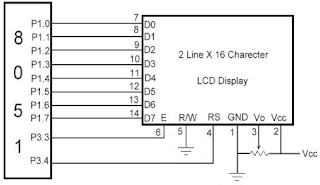
The LCD requires 3 control lines (RS, R/W & EN) & 8 (or 4) data lines. The number on data lines depends on the mode of operation. If operated in 8-bit mode then 8 data lines + 3 control lines i.e. total 11 lines are required. And if operated in 4-bit mode then 4 data lines + 3 control lines i.e. 7 lines are required. How do we decide which mode to use? It’s simple if you have sufficient data lines you can go for 8 bit mode & if there is a time constrain i.e. display should be faster then we have to use 8-bit mode because basically 4-bit mode takes twice as more time as compared to 8-bit mode.
 Pin SymbolFunction
 1 Vss Ground
 2 Vdd Supply Voltage
 3 Vo Contrast Setting
 4 RS Register Select
 5 R/W Read/Write Select
 6 En Chip Enable Signal
 7-14 DB0-DB7 Data Lines
 15 A/Vee Gnd for the backlight
 16 K Vcc for backlight

When RS is low (0), the data is to be treated as a command. When RS is high (1), the data being sent is considered as text data which should be displayed on the screen.
When R/W is low (0), the information on the data bus is being written to the LCD. When RW is high (1), the program is effectively reading from the LCD. Most of the times there is no need to read from the LCD so this line can directly be connected to Gnd thus saving one controller line.
The ENABLE pin is used to latch the data present on the data pins. A HIGH - LOW signal is required to latch the data. The LCD interprets and executes our command at the instant the EN line is brought low. If you never bring EN low, your instruction will never be executed.
For Contrast setting a 10K pot should be used as shown in the figure.
Display Data Ram (DDRAM) stores the display data. So when we have to display a character on LCD we basically write it into DDRAM. For a 2x16 LCD the DDRAM address for first line is from 80h to 8fh & for second line is 0c0h to 0cfh. So if we want to display 'H' on the 7th postion of the first line then we will write it at location 87h.
Now as you have noticed two types of data is given to the LCD data to be displayed, command or special instruction.So now let us write a subroutine for both the type of data

Data to be Displayed

·         lcd_datadisplay:
·         SETB RS                 //Telling the LCD that the data which is being send is to be displayed
·         MOV P1,A              //Character to be displayed is in Acc
·         SETB EN
·         CLR EN                 //High to Low pulse on EN to latch the data
·         CALL DELAY         //Delay so that LCD finishes its internal operations
·         ret 

Command or Special Instruction.

·         lcd_command:
·         CLR RS                   //Telling the LCD that the data which is being send is a command
·         MOV P1,A                           //Character to be displayed is in Acc
·         SETB EN
·         CLR EN                                  //High to Low pulse on EN to latch the data
·         CALL DELAY         //Delay so that LCD finishes its internal operations
·         ret 
Here I have used delay at the end of both the subroutines this is done to wait until the instruction is completely executed by the LCD. This will assure that our program gives the LCD the time it needs to execute instructions and also makes our program compatible with any LCD, regardless of how fast or slow it is.  
"*" - Not Used/Ignored.  This bit can be either "1" or "0" 

Set Cursor Move Direction:

ID - Increment the Cursor After Each Byte Written to Display if Set
S - Shift Display when Byte Written to Display  Enable Display/Cursor
D - Turn Display On(1)/Off(0) C - Turn Cursor On(1)/Off(0)
B - Cursor Blink On(1)/Off(0)  

Move Cursor/Shift Display

SC - Display Shift On(1)/Off(0) RL - Direction of Shift Right(1)/Left(0)  

Set Interface Length

DL - Set Data Interface Length 8(1)/4(0)
N - Number of Display Lines 1(0)/2(1)
F - Character Font 5x10(1)/5x7(0)  
Poll the "Busy Flag" BF - This bit is set while the LCD is processing  
Move Cursor to CGRAM/Display
A - Address 
Read/Write ASCII to the Display
D - Data  
The above Table shows the different commands for the LCD. I wont go into its details.
Before starting to display on LCD we need to Initialize it. Firstly we must tell the LCD whether we'll be using 8-bit or 4-bit mode. Also we will be telling the LCD that we need 5x8 character font. Both these options are selected using a single command i.e. 38h. So to activate both these options we must execute following instructions:
·         MOV A,#38h
·         CALL lcd_command 
Now that we have to Turn On the display & set the cursor option i.e. cursor ON/OFF & Cursor blinking ON/OFF for that we will use the command 0Eh i.e. Display On , Cursor ON but Cursor blinking OFF.
·         MOV A,#0Eh
·         CALL lcd_command 
And the last command we require is to configure the LCD in such a way that everytime we send a character to it the cursor position automatically increments by one & moves to right i.e. 06h.
·         MOV A,#06h
·         CALL lcd_command 
So the lcd_initialize contains the following instructions
·         lcd_initialize:
·         MOV A,#38h
·         CALL lcd_command
·         MOV A,#38h
·         CALL lcd_command
·         MOV A,#38h
·         CALL lcd_command
·         ret 
Similarly another important instruction that we require is Clearing the LCD i.e. 
·         lcd_clr:
·         MOV A,#01h
·         CALL lcd_command
·         ret
Now we know all the commands to display on LCD. Let us write a program that will display 'DNA TECHNOLOGY' on LCD.
·         ORG 0000h
·         CALL lcd_initialize
·         CALL lcd_clr
·         MOV A,#80h //Location from where Data is to be displayed
·         CALL lcd_command
·         MOV A,#'D'
·         CALL lcd_datadisplay
·         MOV A,#'N'
·         CALL lcd_datadisplay
·         MOV A,#'A'
·         CALL lcd_datadisplay
·         MOV A,#20h         //Hex value for blank space to be displayed
·         CALL lcd_datadisplay
·         MOV A,#'T'
·         CALL lcd_datadisplay
·         MOV A,#'E'
·         CALL lcd_datadisplay
·         MOV A,#'C'
·         CALL lcd_datadisplay
·         MOV A,#'H'
·         CALL lcd_datadisplay
·         MOV A,#'N'
·         CALL lcd_datadisplay
·         MOV A,#'O'
·         CALL lcd_datadisplay
·         MOV A,#'L'
·         CALL lcd_datadisplay
·         MOV A,#'O'
·         CALL lcd_datadisplay
·         MOV A,#'G'
·         CALL lcd_datadisplay
·         MOV A,#'Y'
·         CALL lcd_datadisplay
·         stop:
·         ajmp stop 

Debugging Procedure 

If the above program does not work then follow these steps:-
1) Check if the supply is correct.
2) If all connections are correct.
3) Increase the delay time.


Interfacing Matrix Keypad to 8051

Before learning “Interfacing Matrix Keypad to Microcontroller” you should know how to interface a switch to microcontroller for which please click here.
As you have seen in the article for interfacing switches to microcontroller  normally the port pin is high but when a switch is pressed the controller pin gets a Low signal and we come to know that a switch has been pressed. One end of switch is connected to the port pin whereas the other end is connected to the Ground.
In case of matrix Keypad both the ends of switches are connected to the port Pin. Over here we have considered a 4x3 matrix keypad i.e. four rows and three columns. So in all twelve switches have been interfaced using just seven lines. The adjoining figure shows the diagram of a matrix keypad and how it is interfaced with the controller.
As you can see no pin is connected to ground, over here the controller pin itself provides the ground. We pull one of the Column Pins low & check the row pins if any of the Pin is low then we come to know which switch is pressed.
Suppose we make column 1 pin low and while checking the rows we get Row 3 is low then we come to know switch 7 has been pressed.


ALGORITHM

1.       Start.
2.       Make All Pins High.
3.       Make Column 1 pin low.
4.       Check if Row 1 is low, if yes then Switch 1 has been pressed.
5.       Check if Row 2 is low, if yes then Switch 4 has been pressed.
6.       Check if row 3 is low if yes then Switch 7 has been pressed.
7.       Check if row 4 is low if yes then Switch 10 has been pressed.
8.       Make Column 1 Pin high & Column 2 Pin Low.
9.       Check if Row 1 is low, if yes then Switch 2 has been pressed.
10.   Check if Row 2 is low, if yes then Switch 5 has been pressed.
11.   Check if row 3 is low if yes then Switch 8 has been pressed.
12.   Check if row 4 is low if yes then Switch 11 has been pressed.
13.   Make Column 2 Pin high & Column 3 Pin Low.
14.   Check if Row 1 is low, if yes then Switch 3 has been pressed.
15.   Check if Row 2 is low, if yes then Switch 6 has been pressed.
16.   Check if row 3 is low if yes then Switch 9 has been pressed.
17.   Check if row 4 is low if yes then Switch 12 has been pressed.
18.   Make column 3 pin high
19.   Stop

Please make sure at any time only one column Pin should remain Low.


Interfacing Switch to Microcontroller & Switch Debouncing

In 8051 PORT 1, PORT 2 & PORT 3 have internal 10k Pull-up resistors whereas this Pull-up resistor is absent in PORT 0. Hence PORT 1, 2 & 3 can be directly used to interface a switch whereas we have to use an external 10k pull-up resistor for PORT 0 to be used for switch interfacing or for any other input.Figure 1 shows switch interfacing for PORT 1, 2 & 3. Figure 2 shows switch interfacing to PORT 0.

Image
Image
For any  pin to be used as an INPUT PIN a HIGH (1) should be written to the pin if you don’t do this the pin will always be read as LOW.In the above figure when the switch is not pressed the 10k resistor provides the current needed for LOGIC 1 closure of switch provides LOGIC 0 to the controller PIN.Let's write a small program where whenever a switch is pressed a LED is turned ON. Consider that switch is connected to P2.0 & an LED connected to P2.1. 

PROGRAM 1 

ORG 0000h
                SETB P2.0
                SETB P2.1
loop1:
                JB P2.0,loop1
                clr P2.1
loop2:
                JNB P2.0,loop2
                SETB P2.1
                AJMP loop1
 First we initialize the Port Pins that we are using. Since we are using P2.0 as an InputPin we write logic 1 to it (SETB P2.0). We are using PIN P2.1 for LED. Initially LED is turned OFF this is done by pulling the PIN HIGH (check LED interfacing Section).  Now we check if the Switch is pressed or not. So we wait till switch is pressed (loop1: JB P2.0,loop1) as soon as switch is pressed the LED is TURNED ON ( CLR P2.1 ) . Then we wait till the switch to be released (loop2: JNB P2.0, loop2 ) & then we TURN OFF the LED (SETB P2.1). You must have noticed in the above program that the status of the input pin is same as that of Output Pin i.e. if the switch is not PRESSED (HIGH) the Output pin is also HIGH (LED OFF) & when the switch is PRESSED (LOW) the Output pin is also LOW (LED ON) using this logic we can write in another way. 
PROGRAM 2 
ORG 0000h
                SETB P2.1
                SETB P2.0
loop:
                MOV C,P2.0
                MOV P2.1,C
                AJMP loop
 The Output of both the programs will be the same.Now you know the basic concept of switch interfacing. There is a problem in practically interfacing these switches to the controller. In the above case you have considered the switches to be an IDEAL SWITCHwhere when the switch is pressed the controller directly gets LOGIC 0. But practically when a switch is closed the contacts open & close rapidly for about 30ms. This is called as SWITCH BOUNCING. Figure 3 shows its waveform.
Image
As you can see the switch release is clean without any bouncing. When a switch is pressed the contacts open & close for about 20ms. In the above programs the LED will flicker initially when the switch is pressed because of the SWITCH BOUNCING but since the flickering will be very fast & will not be detected by human eye.Even though 20ms is very short time in human terms for a microcontroller it is a very long time. WithoutSWITCH DEBOUNCING the controller will think that the switch was pressed many times.Let us modify PROGRAM 1 & used SWITCH DEBOUNCING in it. 

PROGRAM 3
ORG 0000h
                SETB P2.0
                SETB P2.1
loop1:
                JB P2.0,loop1
                mov R7,#255
deb1_loop1:
                JB P2.0,loop1
                djnz R7,deb1_loop1
                CLR P2.1
loop2:
                JNB P2.0,loop2
                SETB P2.1
                AJMP loop1
 In this modified program the controller waits  for LOGIC 0 ( loop1: JB P2.0,loop1 ) on input pin i.e. P2.0 then loads R7 with 255 now it checks if the input PIN still has LOGIC 0 (  JB P2.0,loop1 ) the controller checks this LOGIC 0 till the value in R7 becomes 0 which in this case is 255 times. If even once the controller detects LOGIC 1 then it exits the debouncing loop & goes back to the main loop ( loop1 ) indicating error in switch press. Basically the code:- 
                mov R7,#255
deb1_loop1:
                JB P2.0,loop1
                djnz R7,deb1_loop1is used for switch debouncing if you think the debounce period is less then use the LOOP WITHIN LOOP TECHNIQUE to check the input pins for more than 255 times. But personally I never had any problems with debouncing using the above code.